
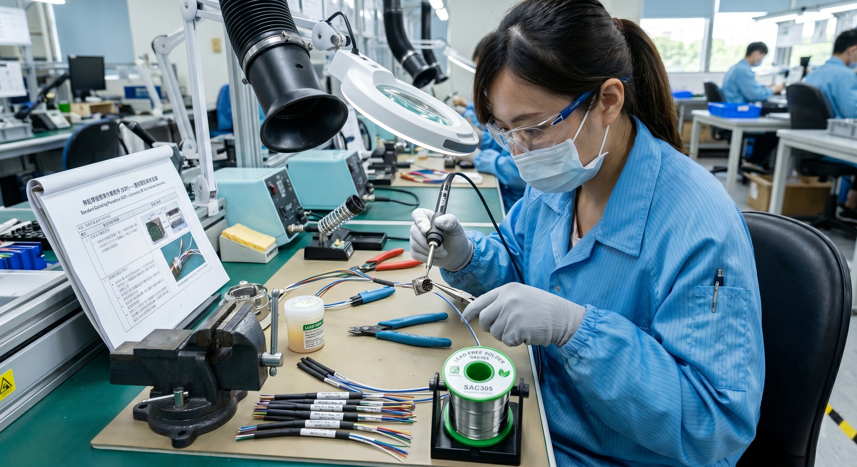
Standard Operating Procedure (SOP) for Lead-Free Soldering: High-Quality Craftsmanship in Connector and Wire Harness Assembly
Driven by the trend toward environmental sustainability in Electronic Manufacturing Services (EMS), lead-free soldering has become a mandatory regulatory standard across the global supply chain. Compared to traditional tin-lead soldering, lead-free processes exhibit a higher melting point and poorer wetting performance, posing significant challenges to the assembly of connectors and precision wire harnesses. This SOP aims to standardize the workflow, ensure solder joints comply with the IPC-A-610 international acceptance standard, and minimize thermal stress damage to electronic components.
1. Pre-operation Check & Environmental Inspection
High-quality soldering begins with a controlled environment. Since lead-free solder is highly sensitive to oxidation, environmental control is the crucial first step to success.
-
Workstation Environment Verification: Check the workstation's temperature and humidity. It is recommended to maintain the temperature at $25 \pm 3^\circ\text{C}$ and the relative humidity (RH) between 40% and 60%. Excessive humidity increases the risk of solder splatter, while insufficient humidity easily generates electrostatic discharge (ESD).
-
Material & Lead-Free Label Verification: Strictly verify that all connectors, wires, and solder materials carry RoHS or LF (Lead-Free) green labels. Mixing with leaded materials is strictly prohibited to prevent cross-contamination, which degrades solder joint strength.
-
Precision Equipment Check:
-
Soldering Iron Temperature Setting: The recommended temperature for lead-free soldering is set between 350°C and 370°C. Fine adjustments can be made based on the solder pad thermal mass, but never exceed 400°C to prevent the excessive growth of the Intermetallic Compound (IMC) layer.
-
Soldering Tip Maintenance: Ensure the tip is free of oxidation or black burnt residues. A dedicated lead-free tip tinner/cleaner must be used, and the tip must be kept well-tinned for protection.
-
2. Flux Application & Precision Solder Feeding Techniques
Lead-free solder has lower fluidity; therefore, precise control of the flux application is key to achieving optimal wetting.
-
Flux Coating Volume Control: Apply an appropriate amount of flux only to the immediate soldering area. Excessive flux leads to corrosive residues or impedance anomalies, while insufficient flux causes poor wetting, resulting in what is commonly known as a "cold solder" joint.
-
Scientific 3-Step Solder Feeding:
-
Preheat: Touch both the connector solder pad and the wire conductor simultaneously with the soldering iron tip to establish a "thermal bridge."
-
Feed Solder: Introduce the lead-free solder wire to the heated junction (Pad/Wire) rather than directly touching it to the iron tip. This ensures the solder is melted by the thermal energy of the materials.
-
Withdraw: Once the solder flows completely and forms a full contour, immediately withdraw the solder wire, followed by the soldering iron. The entire duration should not exceed 3 seconds.
-
3. The Triple-S Stability Law: Core Principles of Soldering
Operators must strictly adhere to the following golden rules during execution, which are vital to ensuring the mechanical strength of the wire harness connection:
-
Speed: The soldering time must be precisely controlled within 2 to 3 seconds. Lead-free solder solidifies slowly, but prolonged high-temperature exposure will cause thermal deformation of the connector plastic housing (e.g., PBT/LCP) or overly thick IMC layers that embrittle the solder joint.
-
Stability: Shaking or movement is absolutely prohibited during the solder joint cooling phase (approximately 3 to 5 seconds). Lead-free solder is extremely fragile during its solidification phase; any micro-vibration will induce stress cracks, creating latent defects for future intermittent open circuits.
-
Shape: An ideal solder joint should exhibit a smooth, uniform, concave fillet shape. Note: A satin or slightly dull matte finish is a normal physical characteristic of lead-free solder joints. As long as the surface is smooth and the coverage is complete, it meets the acceptance criteria.
4. Defect Criteria: The Quality Gatekeeper
In accordance with the IPC-A-610 standard, operators must immediately isolate and report the following soldering defects:
-
Tombstoning & Shifting: Components are not accurately centered or seated properly on the designated target pads.
-
Poor Wetting (Excessive Wetting Angle): The contact angle between the solder and the pad edge exceeds 90°, indicating insufficient thermal energy or surface oxidation.
-
Solder Projections (Spikes/Icicles): Sharp, pointed protrusions on the solder joint surface, which pose a high risk of short-circuiting in high-voltage environments.
-
Charring & Melting: Discoloration or geometric damage to the connector plastic components due to overheating.
5. Post-soldering Processing & Quality Traceability
-
Residue Cleaning: Use high-purity Isopropyl Alcohol (IPA) combined with a lint-free wipe to remove residual flux, ensuring that the areas surrounding the solder joints are free of white residue.
-
First Article Inspection (FAI) & Self-Check Mechanism: Perform a 100% visual inspection on the first 5 pieces of every batch (the use of a 10x magnifier or microscope is highly recommended).
-
Digital Report Logging: Document detailed logs including soldering iron temperature, solder batch number, flux model, and production timestamps. This documentation serves as crucial quality traceability evidence during automotive-grade (IATF 16949) customer audits.
Technical Q&A: Solving Pain Points in Lead-Free Soldering
Q1: Why is lead-free soldering more prone to "bridging" (shorts) than leaded soldering?
A: This is primarily due to the higher surface tension and poorer fluidity of lead-free solder alloys. Solutions include selecting a higher-activity flux and optimizing the soldering iron tip geometry (such as chisel or hoof shapes) specifically for fine-pitch connectors to localize and concentrate thermal transfer.
Q2: How can we prevent "solder balls" from forming during the lead-free soldering process?
A: Solder balls are typically caused by moisture on the pads or the violent vaporization of solvents within the flux. Ensuring that PCBs and wires undergo proper baking and dehumidification prior to assembly, while regulating the solder feeding speed, can significantly minimize solder ball occurrences.
Q3: Why do lead-free solder joints always look dull and gray? Does this count as a defect?
A: No, this is not a defect. It is a normal crystallization phenomenon of lead-free solder alloys (such as SAC305) upon cooling. Quality evaluations must focus on the wetting angle and surface continuity rather than the specular glossiness.
Safety & ESD Protection Protocols
Fume Extraction System: Lead-free fluxes contain more robust activators that produce irritating fumes when heated. High-efficiency fume extractors must be turned on and fully operational throughout the process.
Electrostatic Discharge (ESD) Protection: Connectors are frequently linked to sensitive integrated circuits (ICs). Operators must correctly wear grounded ESD wrist straps, and ensure that the grounding resistance complies strictly with ANSI/ESD S20.20 standards.