
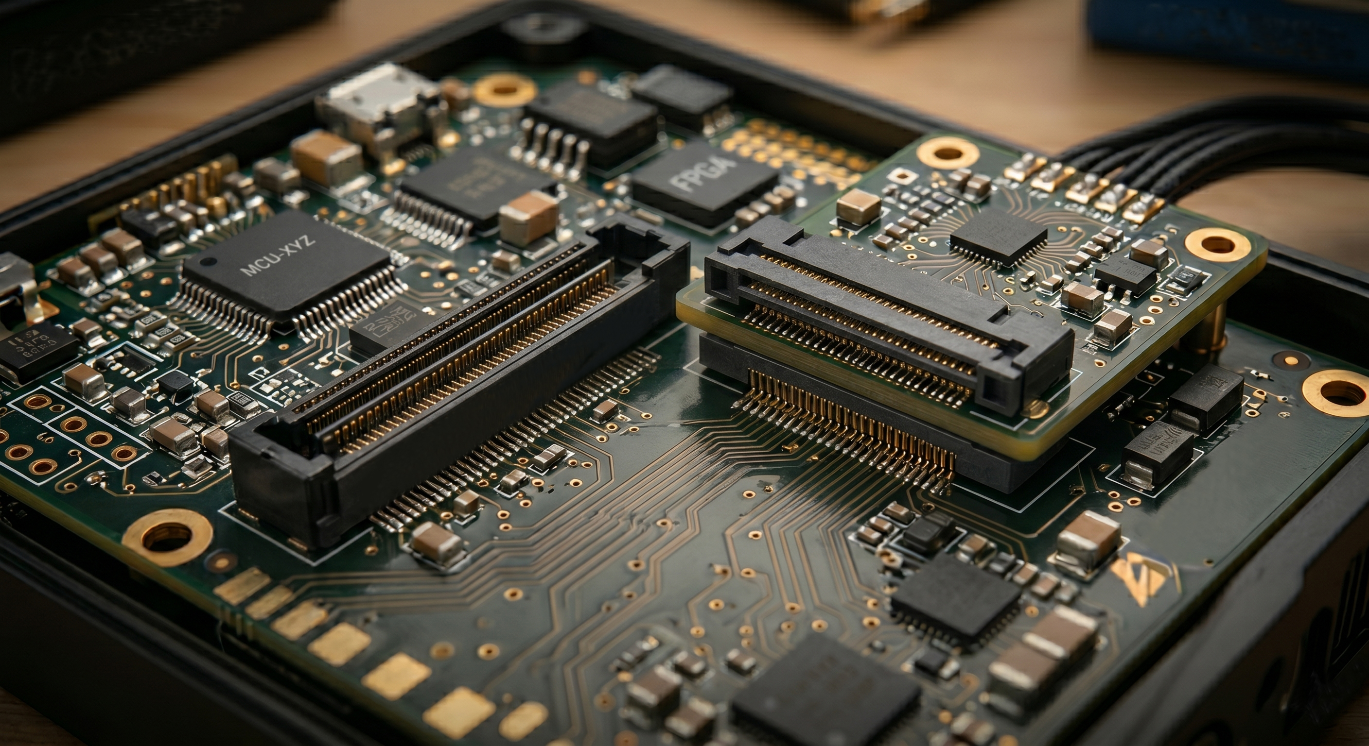
The Space Magic of Microns: Deep Dive into the Hardware Importance and Selection Trade-offs of BTB Connector "Mated Height"
Within the internal, ultra-dense hardware architectures of modern consumer electronics—such as smartphones, smartwatches, and premium wearables—BTB (Board-to-Board) connectors serve as the high-speed signal highways linking the primary motherboard with sub-boards, display panels, touch digitizers, and camera modules. Throughout the PCBA layout phase and component selection process, "Mated Height"—defined as the total vertical clearance of the male plug and female receptacle once fully locked together—is consistently the primary physical parameter considered by hardware architects and layout engineers. Below, we break down the engineering space magic behind mated height selection from both a product marketing and hardware R&D perspective.
I. Dictating Final Product Slimness and Internal Spatial Layouts
In the pursuit of ultra-thin, miniaturized electronics, every single micron (µm) inside the mechanical enclosure becomes a battleground for design engineers.
(I) Cascading Effects on PCB Spacing and Mechanical Clearances
- Defining Board-to-Board Gaps
(1) The mated height of a BTB connector strictly defines the vertical clearance between two parallel PCBs.
(2) Sourcing a connector with an excessively high profile forces an inflation of the final product's thickness, weakening its aesthetic competitiveness in the commercial market.
- Reclaiming Footprint for Battery and Sensor Clusters
(1) By deploying ultra-low profile BTB connectors (such as 0.6mm, 0.8mm, or 0.9mm variants), engineers can compress empty board-to-board dead space to its absolute physical limits.
(2) The reclaimed vertical real estate directly translates into crucial battery pouch capacity or permits the integration of advanced sensor arrays, extending the device's battery runtime.
II. The Engineering Trade-offs of Mechanical Retention Strength
In hardware engineering, however, lower profiles are not universally superior. Mated height selection represents a constant tug-of-war between spatial efficiency and mechanical robustess:
(I) The Mechanical Edge of High-Profile Interconnects
- Extended Effective Contact Areas: Higher connectors typically feature deeper internal metal spring terminal contact points, delivering a significantly higher retention force.
- Superior Drop Test Performance: When the finished device faces severe drop testing or external mechanical shocks, high-profile mated pairs resist microscopic displacements or accidental un-mating failures.
(II) Manufacturing Barriers of Low-Profile Designs
- Compromised Terminal Deflection Travel: Because the vertical height is severely restricted, the physical spring deflection path of the internal terminal contact is truncated. This demands extreme precision in continuous high-speed hardware stamping and plastic injection molding.
- Minimal Tolerance Allocation: During high-volume manufacturing, minor assembly misalignments or uneven SMT solder paste thicknesses can cause low-profile connectors to exhibit poor electrical contact or experience rapid degradation in mating durability.
III. Signal Integrity Optimization and System Thermal Management Clearances
(I) The Impact of Contact Length on High-Frequency Signal Buses
- Shortening the High-Speed Digital Highway
(1) With the rollout of 5G New Radio, millimeter-wave arrays, and high-frequency data buses, the physical length of internal connector pins directly alters signal propagation paths.
(2) Shorter mated heights drastically reduce the electrical path through the contact terminal, minimizing insertion loss, parasitic capacitance, and electromagnetic interference (EMI) in high-speed circuits.
(II) Maintaining Airflow Channels Between Parallel Circuit Boards
- Mitigating Thermal Conduction Risks
(1) When two PCBs are stacked too closely via low-profile connectors, the narrow horizontal gap chokes convective airflow, forcing localized heat dissipation to stall.
(2) Near high-performance Application Processors (APs) or Power Management ICs (PMICs), hardware engineers will occasionally mandate high-profile BTB connectors intentionally to reserve a thermal airflow channel or to allow space for graphite thermal spreaders.
IV. Manufacturing Throughput, Wiping Length, and Factory Assembly Tactility
Mated height selections influence more than early R&D layout boundaries; they directly impact manufacturing throughput on EMS assembly lines:
(I) Wiping Length Capacities and Alignment Tolerances
- Securing the Mating Contact Self-Cleaning Effect
(1) Higher BTB profiles afford a longer wiping length (the distance the male and female terminal pins scrape against one another during insertion). This action shears away surface oxidation layers and micro-dust.
- Pronounced Tactile Feedback (Click Feeling)
(1) Extended mating travel provides assembly operators with a clear, tactile "click" sensation during blind hand-mating.
(2) This immediate physical confirmation helps operators verify that the connector is completely sealed, reducing factory line defects stemming from partial insertions or misalignments, reinforcing proper DFM implementation.
V. Technical Specification Comparison Matrix Across Different BTB Profiles
|
Profile Category |
Standard Height Range |
Core Hardware Advantages |
Primary Engineering Risk & Trade-offs |
Typical Field Applications |
|
Ultra-Low Profile |
0.6mm – 0.9mm |
Extreme Z-axis optimization; ideal for ultra-thin hardware. |
Lower absolute retention force; minimal tolerance for SMT solder variances. |
Smartwatches, main camera modules, ultra-slim OLED display flex cables. |
|
Standard Profile |
1.0mm – 2.0mm |
Balanced mechanical retention and footprint; great tactile feedback. |
Moderate spatial footprint; unsuitable for ultra-miniaturized wearables. |
Main-to-sub board smartphone jumpers, 5G RF antenna sub-boards. |
|
High Profile |
2.5mm and above |
Long contact travel; exceptional shock resistance and superior airflow. |
Bulk footprint; drastically inflates final device thickness. |
Ruggedized industrial handhelds, automotive OBD modules, medical display blocks. |
VI. Professional Technical Q&A: Board-to-Board Mated Height Practical Insights
Q1: When laying out a PCB utilizing an ultra-low-profile (e.g., 0.6mm) BTB connector, what layout safeguards are mandatory?
A: Layout engineers must apply tighter keep-out zones and stricter coplanarity constraints. Because ultra-low-profile connectors allow very little angular misalignment during mating, SMT stencil design must be highly precise to guarantee uniform solder paste deposition. Furthermore, it is highly recommended to integrate physical limit stoppers into the mechanical enclosure immediately adjacent to the connector. This ensures that when the device experiences sudden impacts, the flexing enclosure does not smash down and crush the micro-stamped terminal pins.
Q2: Does the choice of mated height directly alter the current rating of a BTB connector?
A: It exerts an indirect but significant thermal influence. Ultra-low mated heights mean the internal metal terminal blades are severely downsized. Their overall cross-sectional area and physical volume shrink, limiting their thermal dissipation capacity. Consequently, a standard 0.6mm low-profile BTB contact terminal exhibits a modest current rating (typically around 0.3A per pin). If your circuit demands high-current power routing (such as battery power inputs), you must specify a hybrid BTB connector that features dedicated, widened power pins or step up to a higher mated height profile.
VII. Conclusion: Locating the Hardware Architecture "Golden Balance Profile"
Selecting the optimal mated height for a BTB connector is an exercise in space optimization, requiring a deliberate balance between chassis thickness aesthetics, structural mechanical integrity, and assembly plant yields. There is no absolute rule stating that lower is always better; there is only the golden balance profile tailored to a product's precise target market. Driven by advancements in semiconductor processing and micron-scale precision hardware stamping, modern BTB connectors continue to trend toward the frontiers of "ultra-low profile, high-density pin count, and hybrid high-current delivery," redefining physical limitations within the tightest layout footprints.