
From Push-Push to Sink Type: Selecting the Optimal Card Connector Architecture for Diverse Hardware Requirements
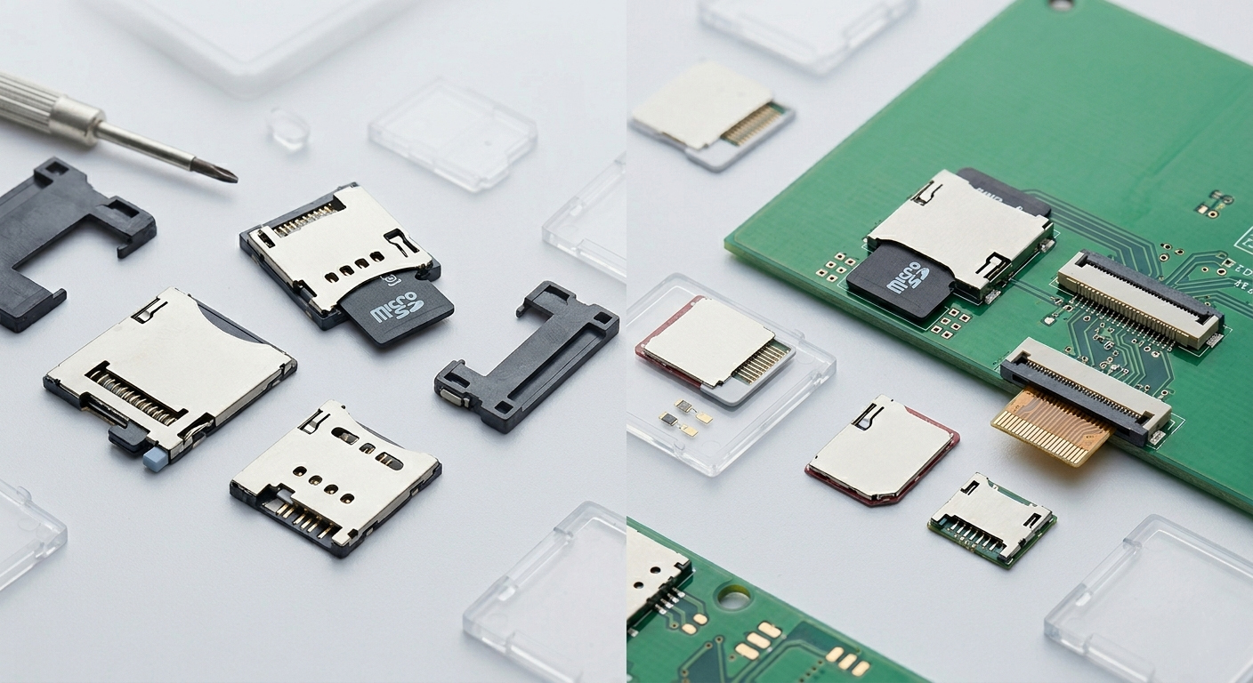
Within the landscape of electronic component sourcing and hardware board design, CARD connectors serve as a vital communication bridge. They manage high-speed parallel data exchanges between external memory or cellular modules and the host printed circuit board assembly (PCBA). Driven by the relentless miniaturization of mobile devices, automotive telematics, and Industrial Internet of Things (IIoT) edge nodes, card slot geometries have diversified significantly. When executing Design for Manufacturability (DFM) and Bill of Materials (BOM) optimization, hardware engineers systematically evaluate and select card connectors across three primary dimensions: form factor specifications, mechanical insertion structures, and PCB mounting methodologies.
I. Classification by "Card Specification": Direct Form Factor Assessment
This foundational classification matrix is governed entirely by the external dimensions, contact pin arrangements, and physical profiles of the targeted media card:
(I) Storage and Cellular Communication Configurations
- SD / Micro SD (TF Card) Connectors
(1) Standard SD Housings: These represent the largest structural footprint, typically incorporating a 9-pin arrangement. Today, they remain baseline configurations for professional DSLR cameras, legacy industrial computers, and high-bitrate video equipment.
(2) Micro SD Housings: Standing as the dominant mass-market volume driver, these carry ultra-compact physical profiles (approximately 11mm x 15mm) outfitted with an 8-pin contact array. They are deployed across smartphones, dashcams, and edge gateways.
- SIM Card Telecom Connectors
(1) Specifically engineered for cellular network tracking, these have scaled down alongside device profiles, transitioning from Micro SIM (3FF) to Nano SIM (4FF). Their interior contacts standardly match a 6-pin or 8-pin mapping.
- High-Integration Combo Card Interfaces
(1) These advanced architectures combine a Micro SD and a Nano SIM slot into a unified housing or implement a dual-option shared mechanical tray. This optimization strategy severely cuts down on dedicated PCB surface real estate (Footprint Optimization).
II. Classification by "Mechanical Insertion Structure": Dictating Usability and Mechanical Clearances
The internal card-retention mechanics define more than the final user's tactile experience; they dictate the connector's internal stress management and structural failure limits:
(I) The Four Primary Mechanical Mating Paradigms
- Push-Push Type (Self-Ejecting)
(1) Technical Features: Integrates an internal precision heart-shaped track, locking pin, and helical spring assembly. A manual push locks the card into position; a secondary push releases the latch, allowing the spring to automatically eject the card.
(2) Engineering Trade-offs: Highly intuitive, requiring zero specialized external tools. However, the spring mechanism occupies a relatively large internal volume. In addition, under sustained industrial harmonics or high-vibration environments (such as automotive chassis), it introduces a severe risk of accidental card ejection.
- Hinge Type (Flip-Top)
(1) Technical Features: Outfitted with a metallic hinged hatch that flips upward. The card is nested inside the nest, and the cover is pressed flat and slid forward into a rigid mechanical lock.
(2) Engineering Trade-offs: Offers exceptional physical shock and vibration resilience, locking the card permanently until manually moved. This makes it the premier choice for automotive electronics, military handheld terminals, and outdoor asset trackers.
- Tray Type (Ejector Pin Style)
(1) Technical Features: Utilizes an independent, removable plastic or metal tray. Ejecting the tray relies on a physical tool or pin entering a dedicated mechanical lever orifice, highly popular in modern unibody smartphone configurations.
(2) Engineering Trade-offs: Complements unibody enclosure designs, permitting superior dust and moisture sealing (IP Rating protection) while maintaining high sleekness. The drawback is its total dependency on an external accessory tray.
- Push-Pull Type (Direct Insertion)
(1) Technical Features: Relies purely on manual force to guide the card in and pull it back out, featuring zero internal spring or lever mechanisms.
(2) Engineering Trade-offs: Features the simplest internal geometry with the lowest component count, ensuring exceptional mechanical durability and low wholesale procurement costs.
III. Classification by "Mounting and Soldering Methodology": PCB Layout Clearances
To accommodate varying PCBA layout clearances and strict vertical Z-axis profile restrictions, card slot mounting configurations are split into three main families:
|
Mounting Profile |
Processing Flow & Geometric Features |
Z-Axis Volume Optimization |
Primary Target Applications |
|
Standard SMT (Top Mount) |
Soldered directly onto the top face of the PCB; represents the most complete standard commodity family in the supply chain. |
Occupies the full vertical height of the connector shell, leaving the bottom layer unaffected. |
Industrial control mainboards, automotive infotainment head-units, bulkier chassis enclosures. |
|
Sink Type (Mid-Mount) |
Requires a pre-milled cutout or slot routed through the PCB substrate, letting the connector body sit "buried" within the board thickness. |
Dramatically compresses vertical Z-height clearance, making it a pinnacle DFM space-saving strategy. |
Ultra-thin laptops, compact smartwatches, and miniature wearable telemetry nodes. |
|
Side Mount (Edge Mount) |
Soldered directly along the physical perimeter of the PCB substrate, with terminal leads standardly bent at a 90º angle. |
Ideal for sleek, low-clearance enclosures requiring side-access card mating. |
Edge-computing IoT gateways, ultra-slim set-top boxes, smart routers. |
IV. Engineering Verification: Metrics to Evaluate High-Quality Card Connectors
When evaluating vendor lines or executing Incoming Quality Control (IQC) procedures, checking a CARD connector's long-term field reliability requires focus on these crucial hardware details:
(I) Plating Thickening, Shell Shielding, and Detection Circuits
- Contact Point Gold Plating Thickness: The gold plating depth over the contact terminal springs (ranging from standard 1µ and 3µ up to premium 15µ) serves as the primary metric determining absolute mating durability cycles and long-term resistance to fretting corrosion.
- Stainless Steel Housings and EMI Shielding: High-tier card connectors utilize heavy-duty stainless steel shells integrated with multiple ground tabs. This provides robust structural crush-resistance and forms an excellent electromagnetic shield, suppressing high-frequency noise emissions during rapid read-write operations.
- Integrated Hardware Detection Switches: Engineers must verify if the connector architecture features an independent mechanical detect pin. Fully seating the card closes or opens this auxiliary loop, alerting system firmware that data read-write operations can proceed safely, mitigating file corruption and data loss.
V. Conclusion
When navigating card connector selection, a proactive approach is the optimal engineering strategy. Layout teams must first isolate the target media card standard, then evaluate the operational environment (e.g., assessing shock vectors versus vertical Z-axis dimensional limits) to balance the choice of mechanical locks and mounting formats (such as hinge type versus sink type designs). Amidst the trend of high-density micro-electronics integration, mastering these subtle geometric parameters locks in factory assembly yields while delivering a reliable, seamless end-user experience.