
The Core of the Slim Revolution: Analyzing Key Applications and Technical Challenges of FPC in the Era of 5G Communications and Edge AI
As 5G millimeter-wave communications, Edge AI, and high-performance edge computing experience explosive growth, the hardware design core of modern electronic products is undergoing a profound metamorphosis—shifting from a pure pursuit of raw computing power to extreme miniaturization and spatial compression. Within this physical hardware revolution, FPC (Flexible Printed Circuit) boards, leveraging their unique physical and electrical attributes, have escalated from basic connecting components to the absolute signaling backbones of device enclosures. This report breaks down the evolutionary path and technical bottlenecks of FPC technology under the twin waves of 5G and AI from both a marketing and materials engineering perspective.
I. What is an FPC? Microstructure and the Three Fundamental Physical Attributes
An FPC is a precision circuit board synthesized utilizing polyimide (PI) or liquid crystal polymer (LCP) polymer films as its flexible base substrate. Compared to legacy Rigid PCBs (RPCBs), it injects three irreplaceable physical properties into Design for Manufacturability (DFM) tracks:
-
Extreme Three-Dimensional Flexing: Capable of unconstrained spatial bending, folding, and twisting, adapting perfectly to the complex 3D mechanical layout inside compact device chassis.
-
High-Density Routing Capabilities: Conductive line widths and spaces can be severely compressed, trimming the absolute volume required by internal circuitry to achieve lightweight device semantics.
-
Premium Convective Thermal Exchange: The ultra-thin physical substrate truncates thermal conduction paths, which is vital for accelerating heat dissipation within tightly sealed, unventilated enclosures.
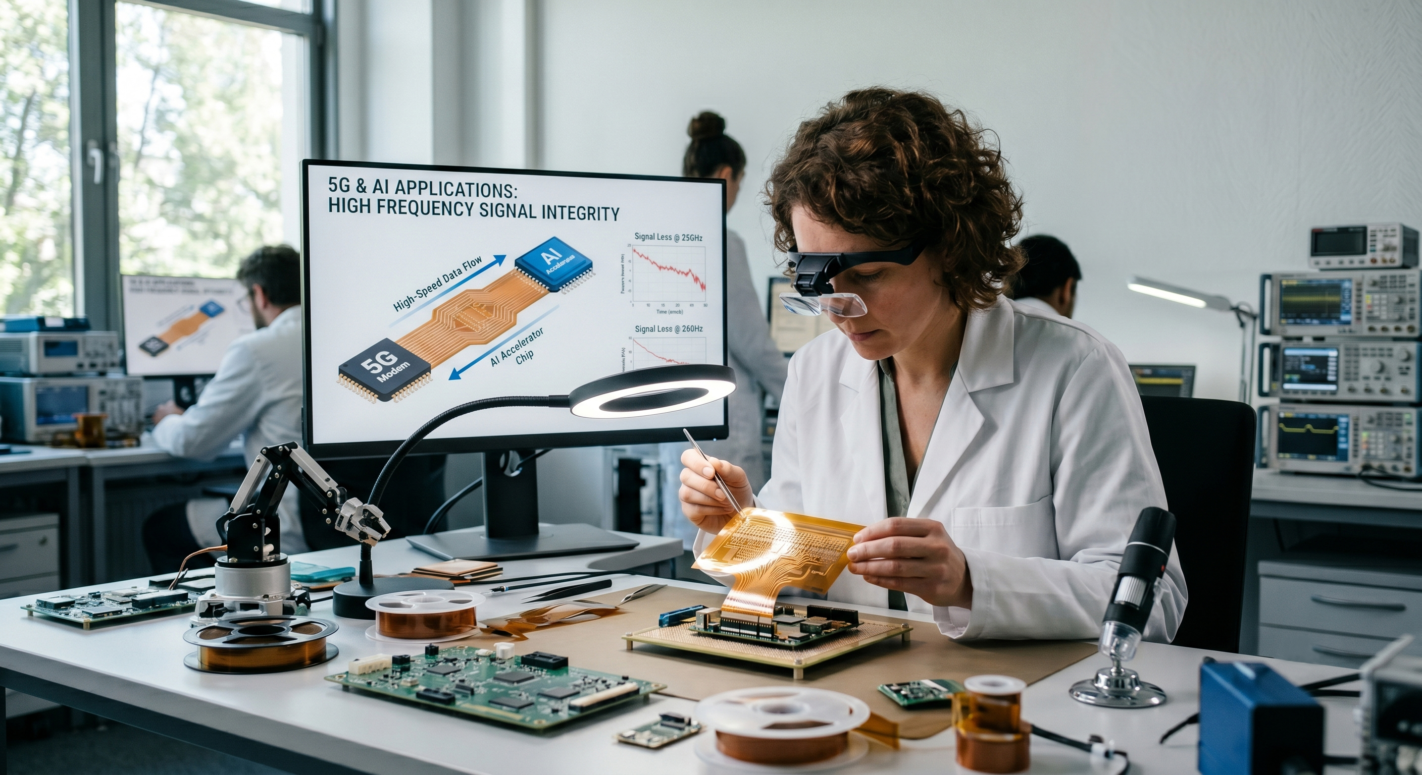
II. The 5G Era: Serving as the "Signal Integrity" Highway for High-Frequency Data Streams
The bedrock of 5G technology relies on high frequency allocations (such as mmWave bands exceeding 28GHz) and ultra-low latency. Within high-frequency electromagnetic propagation paths, minor dielectric absorption triggers severe insertion loss and signal attenuation, which mandates unforgiving electrical performance standards for the underlying FPC substrate metallurgy.
(I) Material Science Evolution and Massive MIMO Array Spatial Layouts
- Transitioning from Legacy PI to MPI and LCP Substrates
(1) Standard polyimide (PI) films exhibit excessively high dielectric constants (Dk) and dissipation factors (Df) when operating at high frequencies, leading to massive transmission losses and localized thermal buildup.
(2) To safeguard signal integrity, 5G FPC architectures have evolved to utilize Modified PI (MPI) and advanced LCP (Liquid Crystal Polymer) compounds, which boast near-zero moisture absorption and pristine, low-loss high-frequency profiles.
- Massive MIMO Antenna Array Consolidation
(1) The proliferation of cellular frequency bands has caused the volume of internal antenna nodes to skyrocket. FPC boards can route dense differential lines across narrow chassis sidewalls or tight corner radiuses, functioning as the premier high-speed highway linking antenna arrays to the primary processor.
III. The Sensory Extension of the AI Era: Multi-Dimensional Implementation of Edge AI
As AI processing scales down from centralized cloud server farms directly into localized end-user devices (such as AI Phones, AI PCs, and smart wearables), the structural application profiles of FPC networks undergo an aggressive evolution:
(II) Smart Wearables, Foldable Displays, and Automotive AI Topologies
- High-Density Wearable Diagnostics and Biometric Telemetry
(1) AI glasses and smartbands require continuous, tight compliance against human skin. The lightweight profile and skin-friendly flexibility of FPCs let high-accuracy biometric sensors blend invisibly into frames or bands, gathering uninterrupted data loops for dynamic AI health analytics.
- The Physical Savior of Foldable Smart Displays
(1) Foldable smartphones represent the vanguard of large-screen Edge AI productivity. The internal FPC interconnects must withstand hundreds of thousands of dynamic bending cycles at tight millimeter radii, while continuously sustaining low-loss data exchanges between the core AI processor and the display panel.
- Automotive AI Intelligent Cockpits and Autonomous Driving Infrastructure
(1) Contemporary electric vehicles (EVs) operate essentially as rolling computing centers. FPC substrates are rapidly replacing traditional, heavy, and space-wasting copper wire harnesses.
(2) By integrating FPCs directly into LiDAR arrays, AI computer-vision camera suites, and smart Battery Management Systems (BMS), carmakers cut down vehicular mass to extend battery range while elevating data bus signaling speeds.
IV. The Four Core Technical Challenges of FPC at the Intersection of 5G and AI
While the high-end flexible electronics sector enjoys expansive market growth, controlling production yields and managing supply chain costs at this technological junction introduce several severe manufacturing barriers:
|
Engineering Dilemma |
Technical Detail & Processing Bottleneck |
Advanced DFM Optimization Strategy |
|
I. Excessive Sourcing Cost |
Synthesizing LCP films involves complex chemical processing, with upstream capacity concentrated among few global suppliers, inflating raw BOM costs. |
Implement supply chain optimizations by flexibly routing MPI (Modified PI) across mid-frequency loops as an authorized equivalent substitute to balance costs. |
|
II. Microscopic Feature Processing |
As AI chip pin densities expand, target FPC line widths and spaces (Line/Space) are pushed toward ultra-fine boundaries under 20µm. |
Transition production lines away from legacy subtractive chemical etching to high-precision mSAP (Modified Semi-Additive Process) to protect assembly yields. |
|
III. Z-Axis Extreme Thermal Ingress |
High-load AI workloads trigger severe thermal dissipation spikes. Heat easily accumulates across ultra-thin FPC surfaces, risking metal trace warping. |
Introduce DFM protocols that embed highly conductive artificial graphite sheets directly into the FPC laminate or widen copper pads at termination joints. |
|
IV. Mechanical Bending Fatigue |
Repeated dynamic articulation across hinge tracks triggers micro-crystalline fractures inside rolled-annealed copper foils, spiking contact resistance. |
Optimize schematic layout geometries; strictly ban 90º sharp turns across bending corridors and reinforce the boundary limits of rigid stiffeners. |
V. Professional Technical Q&A: High-Frequency FPC Manufacturing Realities
Q1: Given that FPC substrates lack structural rigidity due to their ultra-thin profiles, how do automated EMS lines handle precise component component placement and soldering during SMT processing?
A: Managing this factory track depends completely on specialized SMT Carriers / Solder Jigs. Before entering the automated pick-and-place lines, the flexible FPC substrate is tensioned and locked onto a rigid, high-stability backing plate using mechanical locating pins or magnetic clamp downs. This process lets the automated lines interface with the flex circuit as if it were a standard rigid PCB, ensuring precise solder paste deposition and component seating. Furthermore, the carrier material must survive lead-free reflow peak zones reaching 260ºC without experiencing minor physical deflections that distort component coplanarity control.
Q2: Why must the "Coverlay" material of an FPC board undergo a technical upgrade in high-frequency 5G applications?
A: This represents an impedance matching blind spot frequently bypassed by layout designers. Although the outer coverlay (the insulating coat protecting copper traces) does not conduct current, its proximity to high-speed differential lines allows its dielectric attributes to penetrate and alter the surrounding electromagnetic field. If a designer specifies premium, low-loss LCP for the core base substrate but caps it with a legacy, high-loss PI coverlay, high-frequency signaling will still suffer severe surface-wave attenuation. Therefore, in 5G high-frequency designs, the coverlay must be synchronized to low-loss liquid photoimageable (LPI) resins or LCP-grade coverlays to guarantee uniform impedance matching across the transmission channel.
VI. Conclusion
The modern FPC substrate is no longer a simple passive wire routing electrical paths between components; it operates as a core hardware asset dictating 5G transmission stability and refining user experiences at the AI edge terminal. Supported by the maturation of mSAP precision trace lithography and the diversification of multi-source LCP raw material streams, FPC technology will continue to guide hardware architectures toward an invisible, highly intelligent, and ubiquitous future. In this global race toward lightweight computing nodes, organizations that master material science boundaries and control micro-scale manufacturing tolerances will secure long-term market dominance.