
The Digital Highway for the Eyes of Vision: Deep Dive into BTB Connector Selection and Mechanical Kinematics within High-Tier Camera Modules
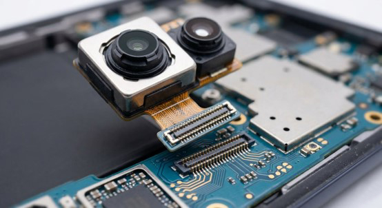
When global technology markets discuss flagship smartphone photography, boasting of "hundred-megapixel" sensors, folded periscope optics, and 8K high-definition video recording, the spotlight almost exclusively lands on the CMOS image sensor and the glass lens elements. However, very few track the narrow digital gate that dictates the success of the entire system—the Camera Module Board-to-Board (BTB) Connector. This micro-scale hardware component operates as an ultra-high-bandwidth interface, directly determining whether the massive real-time data pipelines captured by the CMOS sensor can be transmitted to the Image Signal Processor (ISP) with zero latency and absolute fidelity for Edge AI computing.
I. High-Speed Vision Transmission Bottlenecks: Why Must Camera Modules Specify Advanced BTB Architectures?
Within highly integrated multi-camera matrices and extreme low-profile internal layouts, linking the camera module flex to the main PCBA subjects the interconnect channel to three brutal hardware challenges: high data bandwidths, truncated vertical Z-axis clearances, and volatile electromagnetic interference.
-
Meeting MIPI CSI-2 Protocol High-Speed Bandwidth Demands
(1) Contemporary multi-camera arrays routinely stream massive data feeds measuring multiple Gigabits per second (Gbps).
(2) BTB connectors supply micro-scale physical conduction paths that minimize parasitic capacitance. This design path optimizes Signal Integrity, mitigating high-frequency attenuation, signal reflections, and data lag.
-
Electromagnetic Interference (EMI) Shielding within Micro-Scale Enclosures
(1) The internal CMOS die and voice coil motor (VCM) mechanisms are highly sensitive to high-frequency background noise.
(2) Premium camera-specific BTB connectors feature fully enclosed metal shielding and strategic grounding (GND) anchors to block 5G cellular or Wi-Fi RF noise from corrupting or inducing artifacts into the video frame.
-
Aligning with Design for Manufacturability (DFM) and Modular Servicing
(1) The camera stack represents one of the most expensive sub-assemblies inside mobile electronics and is highly vulnerable to drop impacts. Implementing a mating BTB architecture replaces legacy manual soldering or rigid-flex integration, allowing automated factory lines to achieve rapid assembly while slashing aftermarket repair overhead.
II. The Three Core Technical Metrics of Camera-Specific BTB Connectors
To fit multi-lens configurations inside tight vertical chassis boundaries, connector manufacturers push machining tolerances to the absolute limits of micro-electronics fabrication:
(I) Low Profiles, Dense Pin Counts, and Shielded Framing
- Ultra-Low Profile Mated Heights
(1) To prevent the rear camera bump of the device from expanding excessively, specialized camera BTB interfaces hold their absolute mated heights within a strict 0.6 mm to 0.9 mm boundary. This represents a critical safety metric in precision engineering.
- High Pin Density and Fine Pitch Architecture
(1) A single high-tier camera module requires parallel routing paths for analog power, digital voltages, VCM motor actuation, I²C control buses, and multiple MIPI high-speed differential pairs.
(2) This mandates that the connector squeeze between 20 and 60 precision metal leads into a physical length under 5 mm by employing an ultra-fine 0.35 mm pitch.
- Fully Shielded Structures and Armor Locking Mechanisms
(1) Premium camera BTB solutions implement a fully enclosed metal wrap structure. This metal wrap serves a dual purpose: acting as an EMI ground shield and reinforcing the connector borders via armor-type locks to shield the interior pins from buckling under off-center manual mating stress.
III. Common Hardware Layout Topologies for Mobile Imaging Clusters
Leveraging their high modularity, BTB connectors cleanly support the diverse layout configurations required by contemporary mobile photography:
-
Rear Multi-Camera Matrix Routing
(1) Large-format primary sensors, ultra-wide-angle sub-assemblies, and complex periscope telephoto modules each utilize separate micro-BTB lines to seat precisely onto distinct coordinate anchors across the main motherboard.
-
Front Self-Shot Modules and Extreme Edge Boundaries
(1) Because the vertical and lateral space near the display notch or hole-punch zone is heavily restricted, front-facing camera modules uniquely specify custom ultra-narrow-width BTB connectors.
-
3D Structured Light Arrays and Time-of-Flight (LiDAR) Radar
(1) Face ID authentication modules and laser autofocus setups rely similarly on high-precision, low-impedance BTB connectors to complete millisecond-level depth-map data exchange, ensuring spatial processing suffers zero distortion from interface impedance shift.
IV. Core Specification Comparison Matrix for Camera Interconnect Sourcing
During the New Product Introduction (NPI) track, hardware validation teams must stress-test the camera interface parameters against the following engineering benchmarks:
|
Technical Metric Target |
High-Tier Camera Standard Boundary |
Real-World Engineering Benefit Delivered |
|
Operational Pitch |
Prioritize 0.35mm ultra-fine pitches. |
Maximizes terminal density within localized dimensions to accommodate complex MIPI tracing. |
|
Coplanarity Deviation |
Pin coplanarity must be held under 0.08mm. |
Prevents non-wetting or cold joints during high-speed automated SMT reflow lines. |
|
Wiping Length |
Recommend retaining a minimum of 0.15mm. |
Absorbs physical structural shifts from sudden device drops, preventing signaling drops and screen flickering. |
V. Professional Technical Q&A: Camera BTB Integration and Production Realities
Q1: For ultra-low profile (e.g., 0.6mm) camera BTB connectors, how do tool designers preserve a distinct "Click Feeling" to prevent factory assembly alignment errors?
A: Compressing the vertical profile height of a connector limits the physical wiping length and elastic deflection window of the metal terminals, which can cause the tactile click feeling to fade. To correct this via DFM optimization, tool designers must calculate the geometric ramp angle of the outer metal armor latching channels. High-quality BTBs use these armor locks to trigger a crisp mechanical snap the exact instant the plug aligns and seats into the receptacle. This tactile feedback allows assembly operators to confirm a secure link solely via finger-press feel, eliminating loose-mating field defects.
Q2: Camera BTB interfaces transmit highly sensitive, high-frequency signals. What parameters must be audited when qualifying an alternative second-source drop-in replacement?
A: Because camera BTB pins route fragile differential signal lines, procurement and R&D teams must look past basic footprint alignment during alternative component validation. Engineering teams must evaluate high-frequency impedance matching and insertion lifecycle durability. Sourcing teams should mandate that the alternative vendor provide high-frequency eye diagram reports via a multi-port Network Analyzer. This ensures that after 30 insertion cycles, the contact resistance stays safely below 30mΩ and signal attenuation remains within strict MIPI thresholds, allowing the component to be safely dual-sourced.
VI. Conclusion: The Silent Enabler of Computational Photography
The specialized BTB connector chosen for high-tier camera modules represents the pinnacle of precision manufacturing and micro-scale kinematics. It must simultaneously carry vast digital streams and defend against aggressive electromagnetic interference on densely packed PCBA surfaces. As mobile electronics continue to integrate Edge AI computational photography and multi-axis optical configurations, the camera BTB will evolve toward even lower profiles, wider bandwidth capacities, and fully enclosed armored framing. Mastering the physical tolerances and impedance metrics of this compact interface remains the definitive pathway for hardware teams to push the limits of mobile imaging and guard global brand quality records.