
Transmission Power Hidden at the Fingertips: Deep Dive into Material Science, High-Speed Impedance, and Monolithic Integration of Ultra-Slim USB 3.0 Plugs
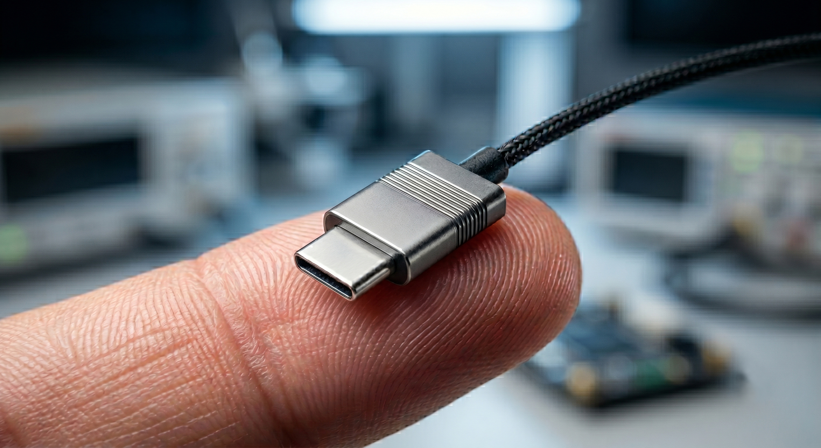
In the relentless race for modern consumer electronics to become ultra-thin, the standard USB interface—with its bulky footprint and rigid metal shell—once stood as a severe bottleneck choking industrial design (ID) breakthroughs. The debut of the Ultra-Slim USB 3.0 Plug / Connector is far more than a basic compression of physical geometry; it represents the absolute intersection of precision micro-electronic engineering, high-frequency electromagnetics, and advanced materials science. This technical analysis breaks down this low-profile interconnection technology through the lenses of structural packaging, signal integrity, and thermal management.
I. The Art of Structural Subtraction: Monolithic Overmolding and Micro-Scale SIP Processes
To slice away more than half the vertical thickness of a standard USB 3.0 interface without compromising electrical conduction, hardware teams must completely abandon the traditional assembly method of wrapping a metal shield over a molded plastic core, pivoting instead to unified Design for Manufacturability (DFM) innovations.
-
Eliminating the Legacy Outer Metal Shell
(1) Advanced ultra-slim plugs adopt a shell-less or ultra-thin secondary Overmolding process.
(2) This fabrication methodology embeds the stamped metal contact pins directly into high-strength reinforced polymer composites, leveraging the physical rigidity of the plastic body to simultaneously handle electrical insulation and mechanical structural reinforcement.
-
Implementing System-in-Package (SIP) Topologies
(1) High-speed control ICs and peripheral passive components (such as decoupling capacitors and ESD protective diodes) are integrated directly onto a miniature multi-layer rigid substrate nested inside the interface cavity.
(2) This packaging evolution shortens the absolute length of the rear plug tail (PCBA termination zone), facilitating extreme micro-miniaturization of the external hardware profile.
II. Safeguarding 5Gbps High-Speed Rails: High-Frequency Impedance Matching and EMI Control
Operating under SuperSpeed architecture, USB 3.0 channels stream massive data loads measuring up to Gbps per lane. The fundamental and harmonic frequencies of these data lines cascade directly around the 2.4GHz band, creating a severe co-channel interference risk for ubiquitous Wi-Fi 2.4G and Bluetooth modules nested inside the same chassis. Because compressing the physical shell limits the available grounding shield clearance, Signal Integrity (SI) confronts unforgiving boundaries:
(I) Characteristic Impedance Calibration and Low-Loss Dielectric Substrates
- Precision Micro-Scale Characteristic Impedance Matching
(1) Within tightly restricted spaces, layout engineers must model and hold the differential pair characteristic impedance (Z0) within a strict safety window of 90Ω ± 7%.
(2) Any micron-scale geometric tooling deviation or solder layer variance triggers heavy return loss and signal reflections, causing eye-diagram closure and severe packet drops.
- Transitioning to Low-Dielectric Constant Polymers
(1) Ultra-slim core insulators substitute standard plastics with premium Liquid Crystal Polymer (LCP), leveraging its low dielectric constant (Dk) and dissipation factor (Df) to curb high-frequency energy decay across the insulating medium.
(2) According to classical electromagnetic physics, high-frequency dielectric loss scales proportionally with transmission frequency and the dielectric loss tangent (tanδ):
Loss ∝ ƒ · tanδ
Slim design configurations must deploy advanced LCP matrices to minimize this tanδ penalty.
III. Dual-Layer Terminal Grid: Balancing Backward Compatibility with Planar Mating Topologies
While pushing physical geometry limits, the ultra-slim USB 3.0 plug must maintain total backward compatibility with legacy USB 2.0 host ports. To reconcile these requirements, the internal terminal configuration deploys a staggered, two-tier contact layout:
|
Contact Allocation Zone |
Target Electrical Signal Definition |
Structural Geometry & Mechanical Contact Attributes |
|
Leading Edge (4 Pins) |
Manages legacy USB 2.0 tracks: VBUS, D-, D+, and GND. |
Ensures electrical conduction loops engage first when sliding into an older legacy host receptacle. |
|
Rear Tier (5 High-Speed Pins) |
Manages USB 3.0 SuperSpeed differential pairs (StdA_SSRX+ and StdA_SSTX-) plus extra ground shields. |
Replaces traditional curved spring contacts with flat pad contacts to optimize vertical Z-axis clearance. |
While pad-style contacts severely compress absolute height, discarding the mechanical suspension clearance of spring cantilevers forces the mating pads to endure harsh, raw sliding friction. To insulate the metallurgy against premature abrasive wear across thousands of insertion cycles, the mating contacts must be treated with a robust 30µ heavy localized gold plating (Heavy Gold Plating) layer to preserve low contact resistance over time.
IV. Extreme Thermal Management and Interference-Fit Mechanical Mating Kinetics
-
Dynamic Thermal Relief in High-Density Clearance Enclosures
(1) Trimming component mass spikes the localized thermal density. When running high-current battery charging tracks via the BC 1.2 protocol or executing continuous high-speed read/write operations, the slim plug lacks the thermal mass of a bulky metallic shell, driving down its natural convective heat dissipation efficiency.
(2) Contemporary precision designs combat this by introducing highly conductive encapsulating resins during the overmolding cycle. These materials act as an efficient thermal bridge, rapidly catching and drawing structural waste heat away from the silicon die out to the cable assembly jacket or device metal frame.
-
The Mechanics of Interference-Fit Mechanical Retention
(1) Lacking the mechanical grounding spring latches found on standard USB shells to deliver retention damping, ultra-slim variants depend on a precise "interference fit" between their polymer geometry and the mating receptacle wall.
(2) Designing the interface with micron-scale dimensional tolerances generates targeted physical friction, supplying adequate retention force to prevent power glitches or accidental disconnects from routine movement.
V. Professional Technical Q&A: Ultra-Slim USB 3.0 Processing and Layout Realities
Q1: Shell-less plugs discard traditional metal grounding wrappers. How do automated manufacturing and assembly lines protect the integrated SIP control chips against Electrostatic Discharge (ESD) failure vectors?
A: This processing vulnerability is common to shell-less geometries. To protect the logic paths via DFM optimization, the internal micro-PCBA must prioritize a dedicated Transient Voltage Suppression (TVS) Diode Array right along the trace periphery. Additionally, shape the leading edge layout to integrate a "first-make, last-break" low-impedance ground lead (GND Pin). Consequently, whether managing static accumulation from automated robotic grip plates or intercepting human handling voltages during field use, the static charge is safely discharged into the primary system ground plane microseconds before the high-speed signaling pairs make electrical contact.
Q2: Cable processing plants frequently encounter adjacent pin bridging or pad delamination when manually soldering multi-strand core lines to compressed ultra-slim plug tails. How can we optimize this?
A: Because the pin configuration matrix on the rear termination zone is heavily compressed, applying manual soldering irons introduces high thermal stress that ruins pads and causes short-circuit bridges. The definitive correction strategy requires transitioning to automated laser welding (Laser Welding), which strictly confines the Heat Affected Zone (HAZ). Following laser termination, mandate a secondary low-pressure epoxy overmolding process. This low-pressure injection fuses the external cable jacket directly to the plug's polymer spine, transferring external pulling strains to the structural outer resin and ensuring zero mechanical load impacts the critical electrical solder joints.
VI. Conclusion
The evolution of the ultra-slim USB 3.0 plug showcases the pinnacle of precision manufacturing—blending complex engineering into an invisible asset. It moves beyond serving merely as a visual styling complement for sleek mobile accessories; it operates as an elegant hardware solution where engineers master high-frequency electromagnetic waves, suppress aggressive EMI noise, and balance thermal densities within a heavily compressed vertical footprint. The successful deployment of this interface detaches high-performance data pipelines and power delivery from the confines of heavy legacy shells, securing a clean digital connection that feels wireless yet performs with high-speed wire stability.